Table of Contents
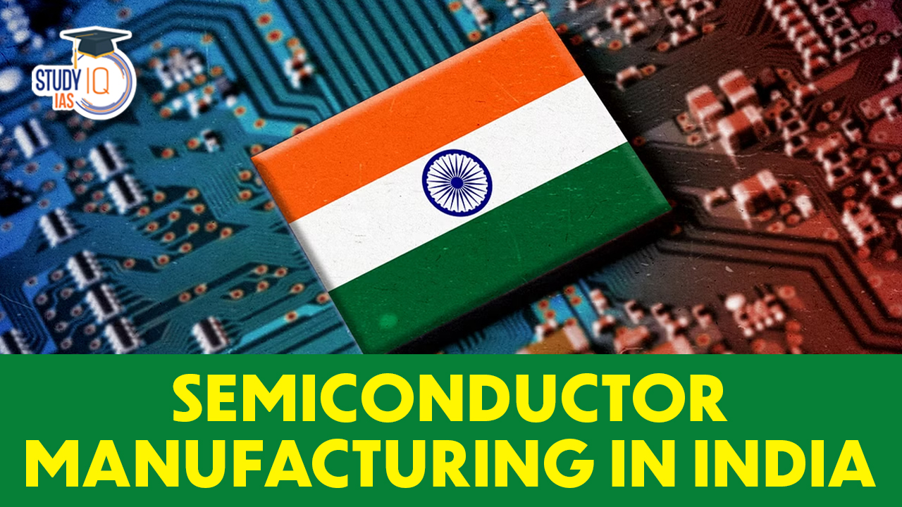
Context: The TATA group has partnered with Taiwan’s Power chip Semiconductor Manufacturing Corporation (PSMC) to set-up a 300mm wafer fabrication plant in Gujarat.
- Semiconductor chip manufacturing is limited to a few regions globally.
- Recent supply chain disruptions and geopolitical tensions highlight the importance of chip manufacturing.
What is a Semiconductor Chip?
- A semiconductor has properties between a conductor (which conducts electricity) and an insulator (which does not).
- In its purest form a semiconductor is a very weak conductor of electricity.
- However, its electrical properties can be changed by adding small amounts of certain substances called ‘dopants’.
- Complex circuits are “printed” on the semiconductor by strategically placing dopants.
What is a Transistor?
- A transistor is a versatile electronic component built using a semiconductor.
- It can function as an electronic switch, amplifier, or part of high-frequency signal circuits.
- Millions/billions of transistors on a chip perform various logical and computational operations.
| Fact |
| Transistors laid the foundation for the semiconductor revolution (Nobel Prizes in 1956 and 2000). |
Fabrication Technology Advancements
- Manufacturing technologies have miniaturised semiconductors significantly.
- Smaller features are achieved using more precise stencils for etching intricate patterns.
- Transistors switch faster and consume less power with each new technology generation (e.g., 45nm, 28nm, 16nm).
- Researchers are exploring using the third dimension (height) to pack more functionality on a chip.
What is a Wafer?
- A wafer is a circular piece of semiconductor material where chip arrays are manufactured.
- Similar to printing many stamps on a sheet of paper before cutting them out individually.
- Larger wafers allow for more chips per production run, reducing cost.
- The current standard wafer size is 300mm (12 inches in diameter), with efforts underway to move to 450mm.
Chip Packaging and Testing
- After dicing the wafer into individual chips, each chip is packaged for protection.
- Tiny wires connect the chip to the package for power, signal, and data.
- Assembly and test plants perform chip functionality verification and stress testing for reliability.
India’s Semiconductor Ecosystem
- India has had a thriving chip design industry since the 1990s using computer-aided design (CAD) tools.
- The existing pool of electronics and computer engineers can support the new focus on manufacturing.
- Semiconductor manufacturing being an essentially inter-disciplinary endeavour, could present opportunities to a wider array of professionals such as process and control engineers, data scientists, material scientists, physicists and chemical engineers to contribute meaningfully to this industry.
Need for Semiconductor Manufacturing in India
- Reducing imports: Taiwan, Singapore, Hong Kong, Thailand, and Vietnam are the only countries from which India imports all of its chips.
- Atmanirbharta: India’s semiconductor industry would benefit domestic businesses by reducing their reliance on imports and by generating income from exports to other nations.
- Drivers of ICT Development: India has to grow its ICT (Information and Communications Technology) industry to take advantage of the fourth industrial revolution. Semiconductors are crucial to this process.
- National Security: They are employed in vital infrastructures that affect national security, including the transmission of power and communications.
- Strategic Autonomy: By reducing India’s reliance on other nations for essential technology, domestic semiconductor manufacturers can increase the country’s strategic independence and lessen its susceptibility to supply chain disruptions.
- The development of the semiconductor and display ecosystem will have a multiplier effect on several economic sectors as it becomes more deeply integrated into the global value chain.
- The modern information age runs on semiconductor chips. They make it possible for electrical devices to compute and control operations that make our lives simpler.
Challenges in Semiconductor Manufacturing in India
- Complex value chain: The chip design component is highly dependent on Research and Development (R&D) and Intellectual Property (IP) protection, and hence extremely expensive.
- Requires Huge investment: Semiconductor manufacturing is a complex, capital and technology-intensive process.
- Lack of cutting-edge technology: India focuses on “lagging-edge” technology nodes in the start to supply to the automotive and appliance sector.
- Raw materials: Semiconductor fabrication requires specific raw materials such as silicon, germanium, gallium arsenide, as well as chemicals and gases, that need to be imported.
- Lack of uninterrupted power and water supply: Manufacturing a single chip requires hundreds of gallons of pure water, which is both difficult and unsustainable for India.
- Global Competition: The United States of America also passed the CHIPS Act last August, providing subsidies of around $280 billion for manufacturing chips in the country. It has also imposed additional restrictions and sanctions on the Chinese semiconductor industry.
- Other Issues: Lack of long-term stable policies, constant price pressure from other global players, ever-changing innovations and rapid changes in technology etc.
Can India become a Semiconductor Manufacturing hub?
- Currently all of the world’s most advanced semiconductor manufacturing capacity—in nodes below 10 nanometers—is concentrated in just two countries South Korea (8%) and Taiwan (92%).
- Skilled Labour: It requires highly skilled labour as the production of semiconductors as the fabrication process is intricate, involves 400- 1400 complex steps and requires highly specialized inputs like commodity chemicals, speciality chemicals as well as many different types of processing and testing equipment and tools, across several stages. For the process, the company requires highly skilled labour.
- The production of semiconductor chips has to be done in clean areas as contaminated air particles could alter the properties of the materials that form the electronic circuits.
- Huge capital investment: Manufacturing of semiconductor chips requires huge investments. Also, since the designs of chips change quite rapidly, these companies always have to invest in acquiring newer technologies to produce the chips.
- For instance, the market leader in the industry, TSMC has announced that it will invest $100 billion in its fabrication plants over the next three years.
Government Action to Boost Semiconductor Manufacturing in India
- India has identified electronics manufacturing as a key sector to boost its growth in the coming years by producing goods not just for the domestic market, but also for exporting to the world.
- Production-Linked Incentives to Attract Electronics Manufacturers
- The government of India approved a $10 billion incentive plan.
- The product-linked incentive plan aims to attract chip and display industries to the country, to make India a major hub for electronics manufacturing.
- The plan is also aimed at reducing reliance on supplies from China, with which India has tense relations.
- It provides uniform fiscal support of 50 per cent of project cost for semiconductor fabs across technology nodes and display manufacturing.
- Semicon India Programme: To foster the growth of the semiconductor and display manufacturing ecosystem in the country.
- It aims to provide financial support to companies investing in semiconductors, display manufacturing and design ecosystem.
- India Semiconductor Mission (ISM): It has been set up as an Independent Business Division within Digital India Corporation to drive long-term strategies for the semiconductor design ecosystem in the country.
- Scheme for Promotion of Manufacturing of Electronic Components and Semiconductors (SPECS): It provides a financial incentive to boost domestic manufacturing and attract large investments in the electronics value chain including electronic components and semiconductors.
- Modified Special Incentive Package Scheme (M-SIPS): M-SIPS provides financial incentives for setting up new semiconductor manufacturing units in the country. Under the scheme, companies can get a subsidy of up to 25% of their capital expenditure.
- SEWFAP: The Semiconductor Wafer FAB Acquisition Program (SEWFAP) provides financial assistance to Indian companies for acquiring semiconductor fabrication facilities (fabs) outside India.
 Operation Amistad: India's Humanitarian ...
 World MSME Day 2026: Theme, History, Sig...
 What is a Seismic Doublet? Venezuela's R...