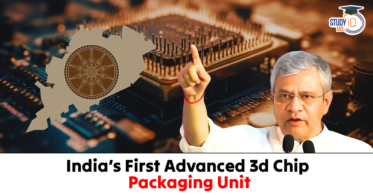
Context: Odisha is setting up India’s first advanced 3D chip packaging unit, marking a step toward high-end semiconductor manufacturing and global supply chain participation.
About the India’s First Advanced 3D Chip Packaging Unit Project
- Implementation: The project is led by 3D Glass Solutions (US-based) through its Indian arm, also funded by Intel.
- Under Government Mission: India Semiconductor Mission (ISM), which supports domestic chip manufacturing.
- Technology: Uses 3D heterogeneous integration, meaning multiple chips are combined into one for better performance.
Ecosystem Significance
- Complete Ecosystem: Odisha becomes the first state with both chip manufacturing (fab) and advanced packaging, strengthening the ecosystem.
- Boost to ATMP/OSAT Sector: Improves India’s role in assembly, testing, marking and packaging, a key part of the chip supply chain.
- Reduced Import Dependence: Less reliance on countries like Taiwan and South Korea for chip processing.
| About 3D Chip Packaging |
In 3D Chip Packaging, instead of placing chips side-by-side, chips are stacked one above another, which saves space and allows faster communication between them.
Key Components
Advantages
|
 Skyroot Vikram-1 Mission Aagaman: India'...
 Oor Pare Prehistoric Site: Location, Roc...
 Assam Election 2026: Exit Poll, Result D...