Table of Contents
Context
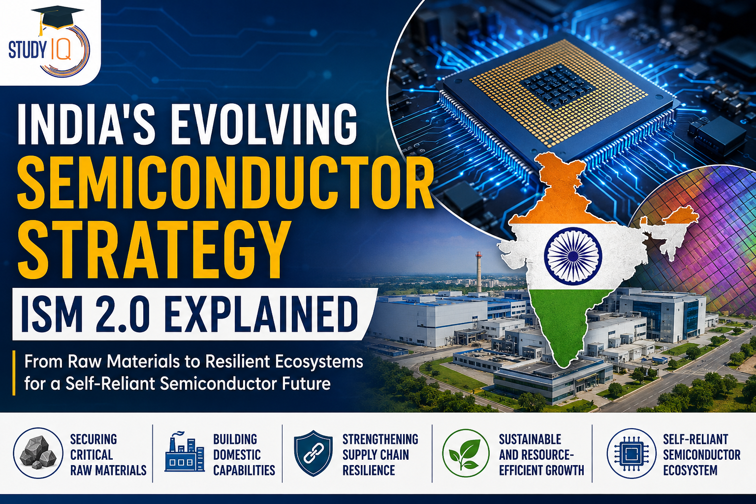
With the Union Cabinet approving the second phase of the India Semiconductor Mission (ISM 2.0) with a total outlay of ₹1.27 lakh crore, India is shifting its focus from merely subsidising chip fabrication to strengthening upstream capabilities, including critical raw materials and refining, to build a resilient and self-reliant semiconductor ecosystem.
Why is India now focusing more on raw materials for making chips, instead of only giving money to build chip factories?
- Incomplete Upstream Support: Although the India Semiconductor Mission subsidises fabrication and assembly, it does not adequately support the upstream ecosystem supplying semiconductor-grade chemicals, gases and wafers, leaving domestic chip manufacturing dependent on imported inputs.
- g., Tata-PSMC’s fabrication plant and Micron’s ATMP facility continue to source most specialty materials from overseas despite receiving government incentives.
- Supply-Chain Risk Mitigation: As domestic manufacturing expands, dependence on a handful of global suppliers for critical inputs such as neon, palladium and photoresists exposes India’s semiconductor ecosystem to geopolitical and supply-chain disruptions.
- g., The 2022 Ukraine war disrupted supplies of semiconductor-grade neon, affecting chip production globally despite fabrication plants remaining operational.
- Strategic Raw Material Security: Since semiconductor raw materials can be stockpiled for long periods without significant quality loss, securing upstream inputs provides greater supply resilience than stockpiling finished chips, which become technologically obsolete quickly.
- g., A strategic neon reserve can keep fabrication plants operational during supply shocks, whereas stockpiled chips lose commercial relevance within a single product cycle.
- Value-Chain Prioritisation: While complete upstream self-sufficiency is desirable, specialty semiconductor chemicals require decades of technological expertise and serve relatively small markets. Industrial policy therefore prioritises scalable manufacturing segments alongside selected upstream capabilities.
- g., The global photoresist and specialty-gas markets are much smaller than the ATMP and legacy-chip manufacturing markets that India can expand more rapidly.
- Targeted Upstream Development: Instead of pursuing self-reliance across every supply-chain bottleneck, policy focuses on upstream segments where India possesses comparative advantages in mining and refining critical minerals.
- g., The National Critical Minerals Mission promotes domestic production of quartz and germanium but does not attempt to localise ASML’s near-monopoly in advanced lithography equipment.
- Beyond Mineral Security: Securing mineral resources alone does not ensure semiconductor self-reliance, as converting them into semiconductor-grade materials requires ultra-high-purity refining technologies that India is still developing.
- g., Quartz and germanium extracted under the National Critical Minerals Mission still require overseas ultra-high-purity refining before they can be used in semiconductor fabrication.
Why are chip factories being set up only in a few states (like Gujarat, Assam, Odisha, Uttar Pradesh and Andhra Pradesh) instead of spreading them across the whole country?
- Agglomeration: Semiconductor manufacturing naturally concentrates into regional clusters because fabs, ATMP units, specialty gas and chemical suppliers, research institutions and skilled workforce benefit from shared infrastructure, lower costs and economies of agglomeration. Many ancillary suppliers must operate close to fabs to ensure safe and timely delivery of highly sensitive materials.
- g., Gujarat has emerged as India’s leading semiconductor hub with Tata-PSMC’s commercial fab, Micron’s ATMP facility and supporting ecosystem investments.
- Fab Infrastructure Requirements: This clustering is reinforced by the fact that commercial wafer fabs require contiguous land, uninterrupted ultra-pure water and highly reliable electricity, restricting viable locations to states with world-class industrial infrastructure.
- g., Gujarat’s Dholera site was selected because of its pre-cleared land bank, dedicated water supply and planned industrial utilities.
- Assembly, Testing, Marking and Packaging (ATMP) Location Flexibility: Unlike wafer fabs, ATMP facilities require relatively less water and power, allowing more states to compete once basic infrastructure is available.
- g., Tata’s semiconductor assembly plant in Assam demonstrates that ATMP facilities can be established outside traditional industrial hubs.
- Air Cargo Connectivity: Even ATMP units depend on the rapid movement of high-value semiconductor materials and finished chips, making proximity to international air cargo hubs essential, while ports primarily support the import of heavy fabrication equipment during project construction.
- g., Uttar Pradesh’s semiconductor ecosystem is expected to benefit from connectivity through the upcoming Jewar International Airport.
- Competitive State Incentives: Where multiple states satisfy infrastructure and logistics requirements, investment decisions are often determined by additional fiscal incentives offered by state governments alongside central support under the India Semiconductor Mission.
- g., Uttar Pradesh’s Semiconductor Policy complements central incentives through state-level capital subsidies, land support and electricity concessions.
- Phased Expansion: Rather than dispersing projects nationwide, India is expanding its semiconductor ecosystem in phases by building on states with established electronics manufacturing capabilities and gradually integrating them into the semiconductor value chain.
- g., Andhra Pradesh is leveraging electronics manufacturing hubs such as Sri City to strengthen downstream integration between semiconductor packaging, electronics assembly and export-oriented manufacturing.
How is India’s semiconductor push redefining industrial policy’s relationship with environmental resource stress?
- Ex-Ante Carrying Capacity Assessment: Instead of treating environmental clearance as a post-approval compliance exercise, industrial policy now evaluates ecological carrying capacity before project approval, ensuring semiconductor investments are located only where long-term water and power availability can be sustained.
- g., The India Semiconductor Mission evaluates water and electricity readiness before extending capital support to semiconductor projects.
- Circular Water Governance: Once projects are confined to environmentally viable locations, policy shifts towards minimising resource consumption through closed-loop water management, making recycling and wastewater recovery integral to industrial planning rather than optional environmental safeguards.
- g., Modern semiconductor fabs increasingly deploy ultra-pure water recovery and Zero Liquid Discharge (ZLD) systems to recycle a substantial share of process water.
- Segment-Level Siting: Since even advanced recycling cannot eliminate differences in regional resource availability, industrial policy aligns different segments of the semiconductor value chain with the ecological carrying capacity of individual states, instead of following a uniform siting strategy.
- g., High-resource wafer fabs are concentrated in infrastructure-intensive locations such as Gujarat, whereas lower-resource ATMP facilities have been established in states like Assam.
- Cross-Sector Resource Allocation: As semiconductor manufacturing competes for scarce water and energy, industrial policy increasingly treats environmental resources as strategic economic assets that must be allocated across industrial, agricultural and domestic users.
- g., Dedicated water conveyance and treatment infrastructure developed for Dholera reflects a deliberate policy decision to allocate scarce water resources to semiconductor manufacturing rather than relying on natural water abundance.
- Resource-Integrated Industrial Planning: This approach is transforming the semiconductor sector into India’s first large-scale model for integrating environmental carrying capacity into industrial planning, creating a template for future resource-intensive industries.
- g., Plug-and-play industrial corridors under the National Industrial Corridor Development Programme increasingly integrate utility planning, environmental readiness and common infrastructure before attracting advanced manufacturing investments.
Read Also: UPSC Daily Current Affairs 2026
 Species in News: Cheetah | Project Cheet...
 Quantum Computing: RRI Scientists Demons...
 Artificial Intelligence in Warfare: How ...














 WhatsApp